
Laser drilling · Microvia PCB
Laser Drilled Microvia PCB: 75 µm Laser Vias for HDI
Laser-drilled microvias from 75 µm connect adjacent layers in HDI build-ups. They can be stacked or staggered and copper-filled where needed, with aspect ratio held at 1:1 and fill and plating verified by microsection.
- Min. laser drill
- 75 µm
- Min. mechanical drill
- 0.10 mm
- Max. aspect ratio
- 1:1
- HDI build-up
- 7-step
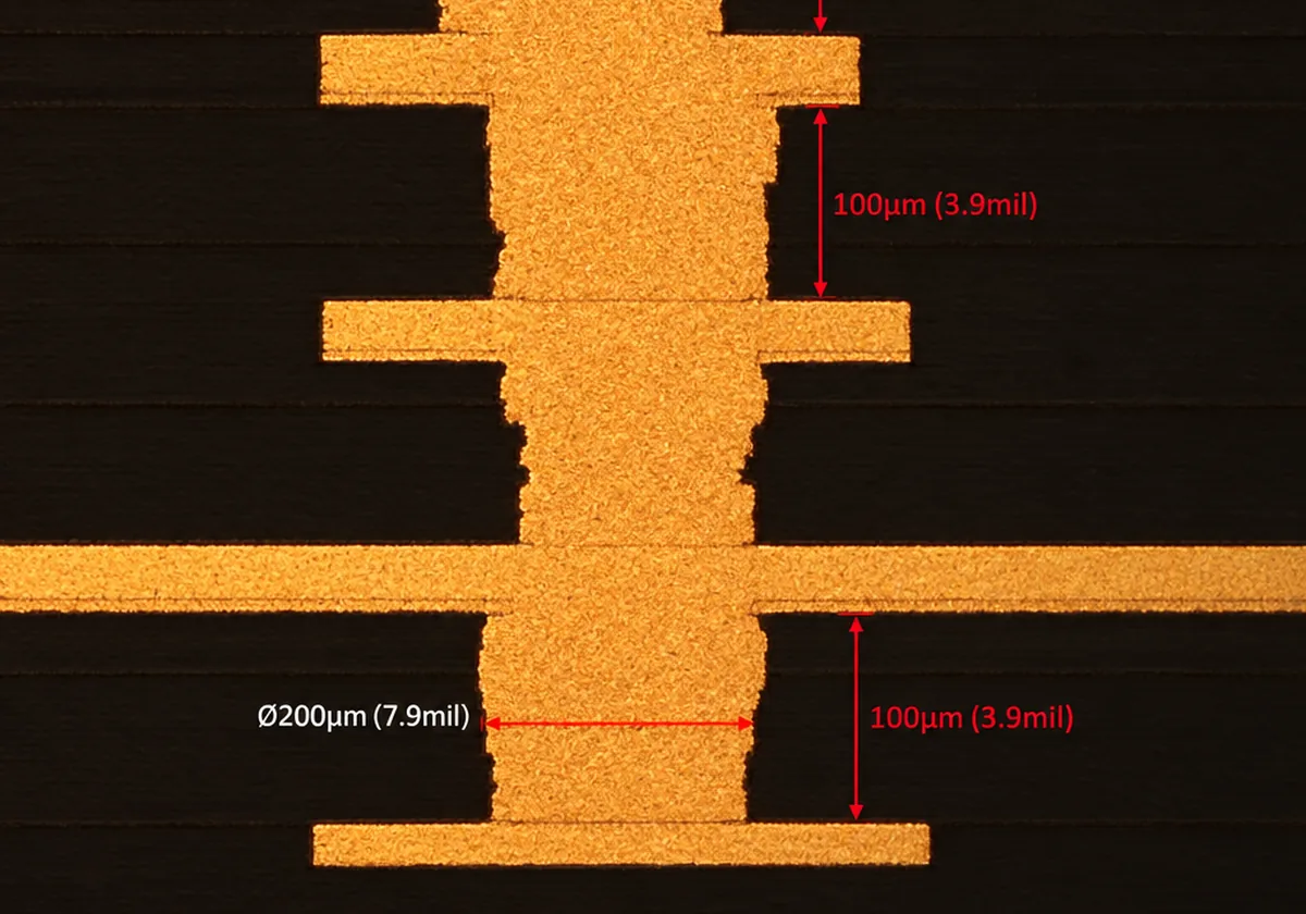
What is a microvia
Microvias, explained.
A microvia is a laser-drilled blind via with a diameter of 150 µm or less that connects one layer to its adjacent layer. It is the building block of HDI PCBs. Microvias take far less pad area than mechanical vias and have almost no stub, which enables 0.4–0.5 mm BGA breakout and clean high-speed transitions.
Microvia diameter, stacking, pad geometry and the surrounding material system have to be decided together with routing density and reliability targets. They are part of the HDI build-up plan, not a separate feature.

Laser drilling
Laser drilling: how microvias are made.
Microvias are formed by UV or CO₂ laser through a thin dielectric layer down to a copper target pad, cleaned by desmear, then copper-plated. UV lasers can ablate copper and dielectric and suit the smallest diameters. CO₂ lasers are efficient for dielectric removal over a pre-opened copper window. Each build-up layer is laminated, drilled and plated in sequence, which is why microvias go hand in hand with sequential lamination.
Specifications
Microvia specifications.
| Parameter | Capability |
|---|---|
| Laser drill diameter | 75 µm minimum laser drill |
| Aspect ratio | Up to 1:1 (depth ≤ diameter) |
| Structures | Stacked (copper-filled) or staggered |
| Build-up | 1+N+1 up to 7+N+7 |
| Fill | Copper fill for stacked and via-in-pad microvias |
| Verification | Microsection and thermal-stress on coupons |
| Mechanical drill (for comparison) | 0.10 mm minimum |
Stacked vs staggered
Stacked or staggered microvias?
| Staggered | Stacked | |
|---|---|---|
| Area | More board area | Least area |
| Cost | Lower | Higher (copper fill each level) |
| Thermal-cycle reliability | Generally more robust | Good when filled; review beyond 2 levels |
| Typical use | 1+N+1, 2+N+2 where space allows | 0.4 mm BGAs, any-layer, SiP |
Stacked microvias connect three or more layers vertically through repeated laser, fill and plate cycles, and each level is copper-filled before the next is drilled. They save the most space, and they are common in 2+N+2 and 3+N+3 boards for phones and SiP packages. Staggered microvias offset each level, which spreads stress and is usually cheaper and more robust in thermal cycling.
In HDI build-ups
Microvias within a 7-step HDI strategy.
We assess microvias as part of the full HDI build-up: laser-drill targets, capture and target pad geometry, stacking sequence, and the fill and cap needs of nearby assembly pads. A 7-step capability does not mean a design should use seven steps. Each extra step adds a lamination cycle, so we look for the fewest steps that route the board. See HDI PCB.
- Document whether each microvia structure is stacked or staggered
- Identify filled and capped via-in-pad locations
- Provide stack-up and electrical requirements before finalizing geometry
Reliability
Microvia reliability.
The weak point of a microvia is the interface between the plated via and its target pad. Poor desmear, thin plating or excessive aspect ratio can leave a weak bond that separates during thermal cycling, often only after assembly. We keep aspect ratio at or below 1:1, control laser cleaning and plating, and verify with microsection and thermal-stress testing on coupons.
- Aspect ratio ≤ 1:1
- Clean target pads (laser desmear)
- Prefer staggered where density allows
- Review 3+ level stacks against thermal cycling
- Microsection on coupons
Design rules
Microvia design rules.
| Item | Typical rule |
|---|---|
| Microvia diameter | 75–100 µm |
| Capture pad | Via + ≈ 100–150 µm |
| Target pad | Via + ≈ 100 µm |
| Dielectric per build-up | ≈ 50–100 µm (≤ via diameter) |
| Via-in-pad | Copper-filled for stacked / BGA |
RFQ
What to include in a microvia RFQ.
- Fabrication data and stack-up intent
- HDI structure (e.g. 2+N+2) and via schedule
- Stacked or staggered, and fill requirements
- Via-in-pad locations
- Reliability or thermal-cycling requirements
- Quantities and schedule
FAQ
Common questions.
What is a microvia in a PCB?
A laser-drilled blind via of 150 µm or less connecting adjacent layers, used in HDI boards.
What is the smallest laser drill you make?
75 µm is our minimum laser-drilled microvia. The minimum mechanical drill is 0.10 mm.
What aspect ratio do microvias need?
Up to 1:1, meaning dielectric depth no greater than via diameter, for reliable plating.
Are stacked microvias reliable?
Yes when copper-filled and designed carefully; stacks beyond two levels need a reliability review.
Microvia vs blind via?
A microvia is a small laser-drilled blind via spanning one layer; blind and buried vias may be mechanically drilled and span several layers. See blind & buried vias.
Do microvias require sequential lamination?
Yes; each build-up layer is laminated, laser-drilled and plated in sequence.
Ready when your files are
Send your design for a capability check.
Upload Gerber, ODB++ or IPC-2581 data. Every quote includes a written engineering DFM review, typically within one business day.