
Case study · Asymmetric HDI · Control systems
Asymmetric HDI PCB Case Study: 14-Layer 2-Step Stacked Vias on Megtron 6
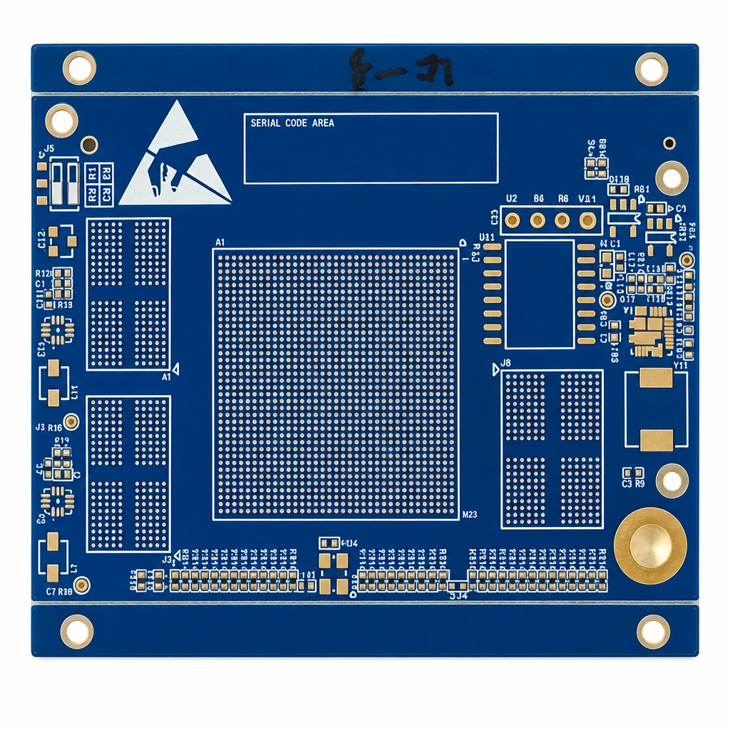
A 14-layer HDI board with an asymmetric 2-step stacked-via structure on Megtron 6, for a compact intelligent broadcast control system. Apart from mounting holes, every outer-layer connection is made with microvias.
- Layer count
- 14 L
- Asymmetric HDI
- 2-step
- Inner hole-to-copper
- 6 mil
- All outer-layer vias
- Microvia
Overview
What this asymmetric HDI project is.
An asymmetric HDI PCB has a different number of build-up layers or via steps on the top and bottom sides, instead of a mirrored structure. This AstroPCB build is a 14-layer Megtron 6 board with 2-step stacked laser vias on the top, multiple blind via spans and all-microvia outer layers.
| Parameter | This build |
|---|---|
| Layer count | 14 layers |
| HDI structure | Asymmetric, 2-step stacked laser vias at L2 |
| Laminate | Panasonic Megtron 6: R-5775G cores, R-5670G prepreg |
| Inner hole-to-copper | 6 mil |
| Outer layers | All microvias except mounting holes |
| End product | Compact intelligent broadcast control system |
| Order range | Samples and small batch |
Key takeaways
- Asymmetric HDI puts build-up layers only where the routing needs them, saving lamination cycles.
- Asymmetry makes warpage control harder, so copper balance and press planning matter more.
- Using microvias for all outer-layer connections frees surface area on a miniaturised board.
The challenge
Why the structure is asymmetric.
The product is a miniaturised control unit, so almost all of the board area was needed for components on the top side. Placing through-holes there would have blocked routing channels and pad space. The design instead moves every outer-layer connection, apart from the mounting holes, into microvias, and adds HDI steps only on the side where the dense BGAs sit.
The result is an asymmetric structure: two laser steps stacked at L2 on the top, a single laser step at the bottom, and multiple blind and buried via spans in between. Asymmetric builds save cost compared with mirroring the build-up on both sides, but they pull the board out of balance during lamination, so flatness becomes the main manufacturing risk.
Stack-up
Stack-up from the production drawing.
| Layers | Material | Thickness | Copper (base → finished) |
|---|---|---|---|
| L1–L2 | R-5670G prepreg, 1078 (68% resin) | 0.089 mm | L1 0.33 → 1 oz |
| L2–L3 | R-5670G prepreg, 1078 (68% resin) | 0.089 mm | L2 0.33 → 1 oz |
| L3–L4 | Megtron 6 R-5775G core | 0.15 mm | 1 / 1 oz |
| L4–L5 | R-5670G prepreg, 1078 | 0.089 mm | L5 0.33 → 1 oz |
| L6–L7, L8–L9 | R-5775G cores | 0.10 mm each | 1 / 1 oz |
| L10–L11, L12–L13 | R-5775G cores | 0.15 mm each | 1 / 1 oz |
| Between cores | R-5670G 1080 (64% resin), two plies | 0.076 mm per ply | — |
| L13–L14 | R-5670G prepreg, 1078 (68% resin) | 0.089 mm | L14 0.33 → 1 oz |
The drawing shows laser vias L1–L2 and L2–L3 stacked on the top, a buried via between L2 and L5, buried vias through the inner core section, a laser via L14–L13 on the bottom and through-holes only for mounting. All core and prepreg materials are from the Megtron 6 family to keep electrical and thermal behaviour consistent.
How we built it
Core manufacturing technologies.
L2 stacked laser vias + multiple blind via spans
Laser vias are stacked at L2 over a buried via, combined with several other blind spans so routing can change layer close to the pads.
Blind & buried viasAll-microvia outer layers
Apart from mounting holes, every outer-layer connection is a microvia, leaving pads and routing channels free on a miniaturised board.
Via in padAsymmetric press control
Lamination profiles and copper balance are planned to limit bow and twist on an unbalanced build.
Multilayer PCBVerification
How builds like this are verified.
- Bow and twist measurement after final lamination
- Microsection of stacked laser vias over the L2–L5 buried via
- Bare-board electrical test (flying probe or fixture) against the netlist
- Impedance coupons measured by TDR where impedance is specified
- Microsection of coupons to confirm microvia fill, plating and layer registration
- Visual and dimensional inspection to IPC-A-600 for the specified class
Design takeaways
When to choose an asymmetric HDI structure.
- Add build-up steps only on the side that needs them; mirroring them both sides adds cost without routing benefit.
- Expect more warpage risk; balance copper area and keep large planes symmetric where you can.
- Tell the fabricator the target bow/twist limit, especially for large BGAs.
- Plan which spans are laser, buried or through-hole before routing; the drill table sets lamination order.
- Keep inner hole-to-copper at or above the agreed minimum (6 mil here).
- Check outer-layer via-in-pad fill and cap requirements for fine-pitch parts.
| Symmetric HDI | Asymmetric HDI | |
|---|---|---|
| Build-up layers | Mirrored both sides | Only where needed |
| Lamination cycles | More | Fewer |
| Warpage risk | Lower | Higher; needs planning |
| Cost | Higher | Often lower |
Quote a similar build
What to send for an asymmetric HDI quote.
- Fabrication data with a drill file per span
- Stack-up with intended build-up per side
- Bow/twist limit and finished thickness
- Impedance targets
- Quantities and schedule
Upload files on the quote page; we return a written DFM and stack-up review.
FAQ
Questions about this build.
What is an asymmetric HDI PCB?
An HDI board with different build-up layers or via steps on the top and bottom, rather than a mirrored structure.
Why choose an asymmetric HDI structure?
To add HDI steps only where routing needs them, which saves lamination cycles and cost on boards with dense parts on one side.
Does asymmetry cause warpage?
It raises the risk. Copper balance, material choice and press profiles are planned to keep bow and twist within limits.
What laminate was used?
Panasonic Megtron 6: R-5775G cores and R-5670G prepregs in 1078 and 1080 glass styles.
Why use microvias for all outer-layer connections?
It keeps through-holes off the outer layers, freeing pad and routing space on a miniaturised board; only mounting holes are through-holes.
What was the inner hole-to-copper spacing?
6 mil.
What quantities do you build?
Samples and small batches for this board type.
Ready when your files are
Building a similar board? Send it for a stack-up review.
Upload Gerber, ODB++ or IPC-2581 data. Every quote includes a written engineering DFM review, typically within one business day.