
PCB design service · Layout & stack-up engineering
PCB Design Service: Layouts Engineered to Be Built
Schematic review, library creation, layout, stack-up and impedance planning, and SI/PI review by designers who work inside a PCB manufacturer.
- Layers designed
- 2–20+
- Allegro · KiCad
- Altium
- Before data exchange
- NDA
- Built in
- DFM
Overview
Design and fabrication under one roof.
A PCB design service turns a schematic into a manufacturing-ready layout: component libraries, placement, routing, stack-up, impedance, rule checks and fabrication outputs (Gerber, ODB++ or IPC-2581). Ours is delivered by designers inside a PCB manufacturer, so every decision accounts for fabrication and assembly limits.
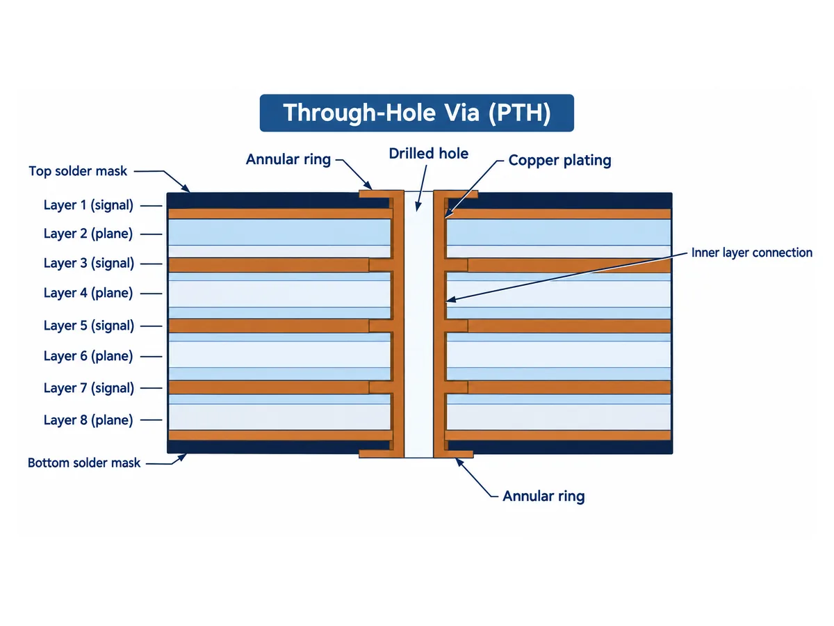
Stand-alone layouts often look right in the EDA tool but need changes before fabrication: annular rings too small for the drill class, impedance geometries the stack-up cannot hit, or via structures that add unplanned lamination cycles. Designing next to the CAM team removes those surprises.
Scope
What the PCB design service covers.
- Schematic review and component selection support
- Library creation with manufacturer-verified footprints
- Placement for signal flow, thermal and assembly
- Impedance-controlled, length-matched routing
- Stack-up design and impedance planning
- Signal and power integrity review
- DRC, DFM and DFA checks
- Gerber, ODB++, IPC-2581, drill, BOM and centroid outputs
DFM built in
Layouts that pass DFM first time.
Because our designers sit next to fabrication, rules come from the production line: real drill-to-copper, annular ring and registration tolerances, available laminate thicknesses and the lamination sequence your via plan implies. You receive the layout with a manufacturing-ready stack-up and a quote path to prototype.
Process
How a design project runs.
NDA & inputs
Schematic, BOM, mechanical outline and constraints.
Stack-up & placement
Agreed before routing starts.
Routing & review
SI/PI and DFM checks with your sign-off.
Outputs & build
Fabrication package and optional prototype.
From schematic to layout
From schematic to layout.
We start from your schematic, whether it is a finished Altium or KiCad project or a marked-up concept with chosen parts. We review it for completeness, confirm footprint availability and critical-net requirements (impedance, differential pairs, power distribution), and build manufacturer-verified footprints for any parts not already in the library.
Layout runs through placement, routing, power-integrity review and DRC. Placement accounts for signal flow, thermal management, assembly sequence and mechanical limits such as connector positions, mounting holes and keep-outs. Routing follows impedance-controlled geometries, length-matches differential pairs and buses, and sizes power shapes for the current, with decoupling placed for the actual PDN.
Typical project timeline
Typical project timeline.
| Board type | Typical layout time |
|---|---|
| 2–4 layer, moderate density | ≈ 1–2 weeks |
| 6–10 layer with impedance control | ≈ 2–4 weeks |
| 12+ layer high-speed or HDI | ≈ 4–8 weeks |
Every project includes agreed review points (stack-up, placement and pre-release) so you can approve the direction before routing effort is spent.
Deliverables
What you receive.
- Native EDA project (Altium / Allegro / KiCad)
- Gerber X2 or ODB++ / IPC-2581 fabrication outputs
- Drill files, fabrication and assembly drawings
- BOM and centroid / pick-and-place
- Stack-up and impedance report
- Optional prototype build — PCB prototype
Why design with a manufacturer
Why design with a PCB manufacturer.
Stand-alone layouts often look right in the EDA tool but need changes before fabrication: annular rings too small for the drill class, trace-to-edge clearance that fails routing or V-score rules, via structures that need unplanned lamination cycles, or impedance geometries the stack-up cannot hit. Designing next to the CAM team removes those surprises, so the first prototype is built as drawn.
Pricing
What PCB design costs.
Simple 2–4 layer layouts typically start around $300–800. Complex multilayer boards with impedance control and high-speed routing usually run $1,000–5,000+. Every project is quoted after we review the schematic and requirements.
FAQ
PCB design service questions.
What does your PCB design service include?
Schematic review, library creation, layout, stack-up and impedance planning, SI/PI review, DFM checks and fabrication outputs.
Which EDA tools do you use?
Altium Designer, Cadence Allegro and KiCad.
How much does PCB design cost?
About $300–800 for simple 2–4 layer boards and $1,000–5,000+ for complex high-speed multilayer designs, quoted per project.
Do you sign NDAs?
Yes. A mutual NDA is signed before any proprietary data is exchanged, and files are stored on access-controlled servers.
Can you fabricate and assemble the board too?
Yes — design flows straight into prototype, fabrication and assembly.
How long does PCB layout take?
About 1–2 weeks for simple 2–4 layer boards and 4–8 weeks for complex high-speed or HDI designs, with agreed review points.
Ready when your files are
Tell us about your design project.
Send your schematic, BOM and mechanical constraints. We reply with scope, schedule and a fixed quote after signing an NDA.