
Case study · Automotive · Megtron 6
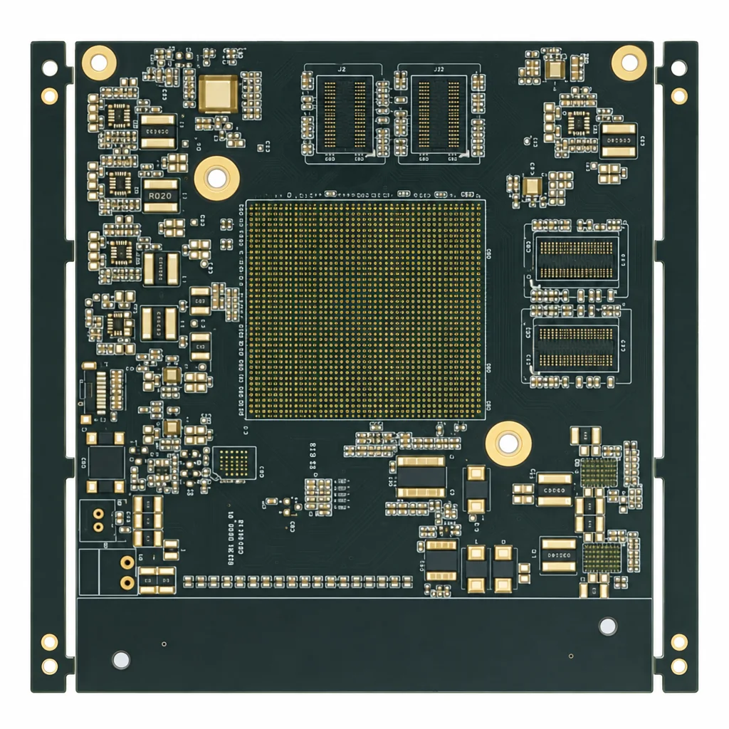
Automotive HDI PCB Case Study: 16-Layer 4-Step Stacked Microvias on Megtron 6
A 16-layer, 4-step stacked-via HDI board on Panasonic Megtron 6 for an automotive intelligent control system, with 6.5 mil inner hole-to-copper spacing and zero open-circuit repair allowed on inner or outer layers.
- Layer count
- 16 L
- HDI structure
- 4+8+4
- Inner hole-to-copper
- 6.5 mil
- Finished ±10%
- 1.8 mm
Overview
What this automotive HDI project is.
An automotive HDI PCB uses laser microvias and sequential lamination to fit high-speed processors into vehicle control units while meeting automotive reliability. This AstroPCB build is a 16-layer, 4-step stacked HDI board on Megtron 6 with 6.5 mil inner hole-to-copper spacing and no open-circuit repair allowed.
| Parameter | This build |
|---|---|
| Layer count | 16 layers |
| HDI structure | 4-step stacked microvias, 4+8+4 |
| Laminate | Panasonic Megtron 6: R-5775G cores, R-5670G prepreg |
| Inner hole-to-copper | 6.5 mil |
| Repair rule | No open-circuit repair on inner or outer layers |
| Finished thickness | 1.8 mm ±10% |
| End product | Automotive intelligent control system |
| Order range | Samples and small batch |
Key takeaways
- Four build-up layers per side over an 8-layer core give a 4+8+4 structure with fully stacked microvias.
- Megtron 6 was chosen for high-speed channels in a vehicle control unit.
- A no-repair rule means every open on any layer scraps the board, so imaging and etching must be right first time.
The challenge
Why this build was demanding.
Intelligent vehicle control units now carry large BGAs, high-speed memory and SerDes links, which is why their boards are moving from through-hole multilayers to HDI. This project combined a 4-step stacked structure, a high-speed laminate and automotive-grade acceptance rules.
Two customer rules raised the bar. Inner hole-to-copper spacing of 6.5 mil leaves little room for drill wander and registration error across multiple presses. And open-circuit repair (re-joining a broken trace) was not allowed on any layer, so any defect after etching meant the board was rejected rather than repaired.
Stack-up
Stack-up from the production drawing.
| Layers | Role | Material | Copper (base → finished) |
|---|---|---|---|
| L1–L4 | Top build-up, laser microvias L1→L2→L3→L4 | R-5670G prepreg, 1080 (68% resin) | 0.33 oz → 1 oz |
| L4–L5 | Bond to core | R-5670G prepreg, 1035 (73% resin) | — |
| L5–L12 | 8-layer core of R-5775G cores (0.075 mm) | Megtron 6 R-5775G + R-5670G 1035 bonds | 0.5 / 1 / 1 / 0.5 oz |
| L12–L13 | Bond to core | R-5670G prepreg, 1035 (73% resin) | — |
| L13–L16 | Bottom build-up, laser microvias L16→L15→L14→L13 | R-5670G prepreg, 1080 (68% resin) | 0.33 oz → 1 oz |
The drawing notes call for 1080 prepreg with 68% resin content on the build-up layers and fresh prepreg stock because the board has blind and buried vias. High resin content fills the copper pattern and the buried via holes without voids, which matters on a board pressed several times.
How we built it
Core manufacturing technologies.
Multi-cycle stacked-via lamination alignment
Each of the four build-up cycles is aligned to the last so stacked microvias land on filled vias below; scaling is compensated per press.
MicroviaAny-layer microvia interconnection
Copper-filled laser vias can be stacked across all four build-up levels, giving direct L1–L4 and L13–L16 connections.
Blind & buried viasRight-first-time imaging
With no open repair allowed, imaging, etching and AOI are controlled so defects are prevented rather than fixed.
HDI PCBVerification
How builds like this are verified.
- AOI of every inner and outer layer; no open-circuit repair accepted
- Microsection of stacked microvias and hole-to-copper spacing
- Bare-board electrical test (flying probe or fixture) against the netlist
- Impedance coupons measured by TDR where impedance is specified
- Microsection of coupons to confirm microvia fill, plating and layer registration
- Visual and dimensional inspection to IPC-A-600 for the specified class
Design takeaways
Design notes for automotive HDI boards.
- Agree the HDI structure (e.g. 4+8+4) before routing; it sets lamination count and cost.
- State hole-to-copper minimums and repair rules on the fab drawing so they are quoted correctly.
- Use staggered instead of stacked microvias where routing allows; staggered vias are more robust in thermal cycling.
- Choose laminate for both signal loss and automotive temperature range.
- Balance copper on build-up layers to control warpage on a 1.8 mm board.
- Plan IPC Class 3 or automotive acceptance criteria and PPAP needs during quoting.
More on vehicle electronics: automotive PCB and Megtron laminates.
Quote a similar build
What to send for an automotive HDI quote.
- Fabrication data with drill files per via span
- Stack-up intent, laminate and finished thickness
- Hole-to-copper and repair rules
- Impedance targets
- Acceptance class, PPAP or traceability needs, and quantities
Upload files on the quote page for a written DFM review.
FAQ
Questions about this build.
What is a 4-step HDI PCB?
A board with four sequential build-up layers on each side of the core, each connected by laser microvias. On this 16-layer board that gives a 4+8+4 structure.
Why use Megtron 6 for an automotive controller?
Megtron 6 is a low-loss laminate for high-speed channels; vehicle controllers with SerDes and fast memory benefit from its lower loss.
What does 6.5 mil inner hole-to-copper mean?
The minimum spacing between a drilled hole and unrelated copper on inner layers. Tight spacing needs accurate drilling and registration.
Why is open-circuit repair not allowed?
Repaired traces are a reliability risk in automotive use, so the customer required every layer to be defect-free without repair.
Are stacked microvias reliable in automotive use?
They can be when fill, plating and lamination are controlled; staggered vias are more robust where routing allows.
What was the finished thickness?
1.8 mm ±10%, with a calculated press thickness of about 1.72 mm before plating and finishing.
What quantities do you build?
Samples and small batches for this board type.
Ready when your files are
Building a similar board? Send it for a stack-up review.
Upload Gerber, ODB++ or IPC-2581 data. Every quote includes a written engineering DFM review, typically within one business day.