
Case study · Heavy copper HDI · Automotive battery
Heavy Copper HDI PCB Case Study: 12-Layer 3 oz High-Tg Board with Crossed Blind & Buried Vias
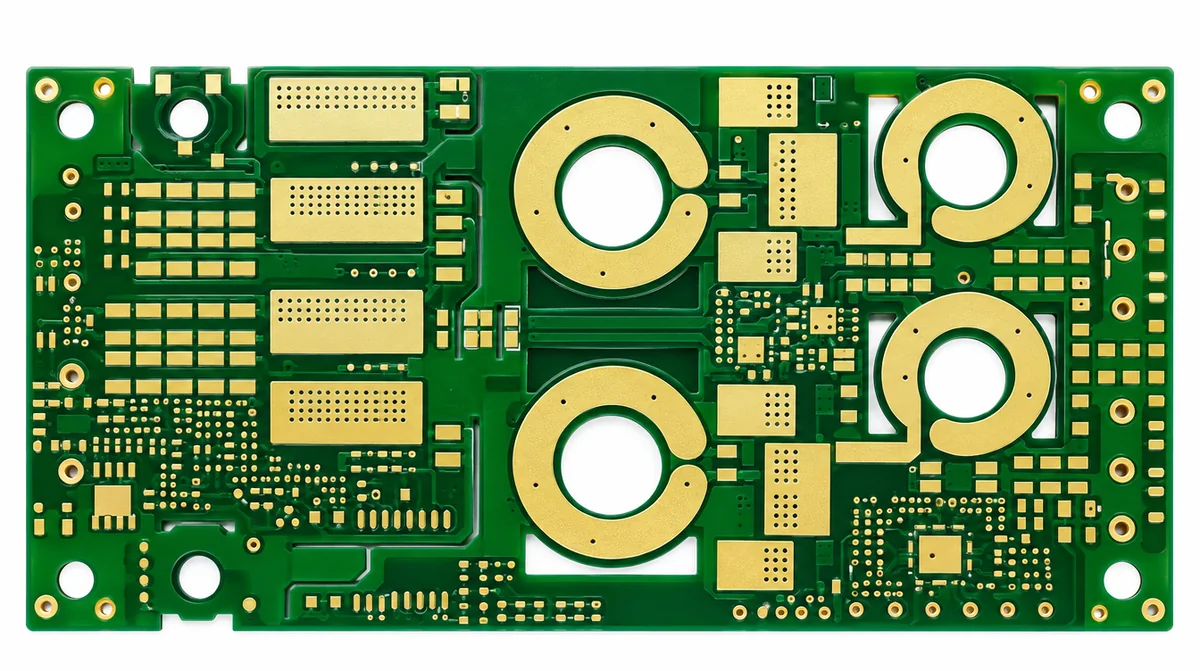
A 12-layer high-Tg FR-4 HDI board for automotive battery electronics, with 3 oz copper on all ten inner layers and laser vias drilled through multiple prepreg plies to create crossed blind and buried via structures.
- Layer count
- 12 L
- Inner copper L2–L11
- 3 oz
- FR-4 S1000-2
- High Tg
- Calculated thickness
- ≈3.2 mm
Overview
What this heavy copper HDI project is.
A heavy copper HDI PCB combines thick copper (typically 3 oz or more) for current with laser microvias for dense routing. This AstroPCB build is a 12-layer high-Tg FR-4 board with 3 oz copper on ten inner layers and laser vias drilled through several prepreg plies to form crossed blind and buried vias.
| Parameter | This build |
|---|---|
| Layer count | 12 layers |
| Laminate | High-Tg FR-4: S1000-2 cores (0.4 mm), 106 prepreg (0.05 mm per ply) |
| Inner copper | 3 oz on L2–L11, ≈60% residual copper |
| Outer copper | 0.5 oz base → 1.5 oz finished |
| Via structure | Laser vias through multiple prepreg plies; crossed blind and buried vias |
| Calculated press thickness | ≈3.2 mm (stack-up calculation) |
| End product | Automotive battery electronics |
Key takeaways
- Ten 3 oz inner layers carry battery-level current while laser vias keep the control circuitry dense.
- Heavy copper needs several plies of high-resin prepreg between layers; here the laser vias are drilled through those multiple plies.
- High-Tg FR-4 handles the heat of high current and repeated soldering.
The challenge
Why heavy copper and HDI on one board is hard.
Battery electronics put power and control on the same board: thick copper carries pack or module current through planes and busbar-like pads, while microcontrollers, monitor ICs and gate drivers need fine routing. Splitting them onto separate boards adds connectors, size and failure points.
Heavy copper and HDI pull in opposite directions. Thick 3 oz copper needs plenty of prepreg resin to fill the gaps between traces, so each dielectric layer is built from several prepreg plies (four plies of 106 between most layers here). Laser drilling has to go cleanly through that thicker, multi-ply dielectric and still plate reliably, and the pressed board ends up around 3.2 mm thick.
Stack-up
Stack-up from the production drawing.
| Layers | Material | Copper (base / finished) | Residual copper |
|---|---|---|---|
| L1 / L12 (outer) | 3 × 10⁶ prepreg (0.05 mm each) to L2 / L11 | 0.5 oz / 1.5 oz | — |
| L2–L3 | 4 × 10⁶ prepreg (high-Tg) | 3 oz / 3 oz | 60% |
| L3–L4, L5–L6, L7–L8, L9–L10 | S1000-2 high-Tg FR-4 core, 0.4 mm | 3 oz / 3 oz | 60% |
| Between cores | 4 × 10⁶ prepreg (high-Tg) | 3 oz / 3 oz | 60% |
| L10–L11 | 4 × 10⁶ prepreg (high-Tg) | 3 oz / 3 oz | 60% |
The drawing shows laser vias from L1 to L2 and from L12 to L11 through three plies of 106 prepreg, a buried via from L2 to L11 through the core stack, and through-holes. Because blind and buried spans overlap in the same area, the structure is described as crossed (interleaved) blind and buried vias.
How we built it
Core manufacturing technologies.
Laser drilling through multiple prepreg plies
Laser parameters are set for a thicker, multi-ply glass-and-resin dielectric so the via is clean, fully open at the target pad and platable.
Microvia3 oz inner layer etching and fill
Thick copper is etched with compensation for undercut, and high-resin 106 prepreg fills between 3 oz features without voids.
Heavy copperCrossed blind and buried vias
Buried L2–L11 vias are drilled and plated before the outer laminations, then laser vias connect the outer layers, in the right sequence.
Blind & buried viasVerification
How builds like this are verified.
- Microsection of laser vias through multi-ply prepreg and of buried via plating
- Checks for resin fill between 3 oz features (no voids or starvation)
- Bare-board electrical test (flying probe or fixture) against the netlist
- Impedance coupons measured by TDR where impedance is specified
- Microsection of coupons to confirm microvia fill, plating and layer registration
- Visual and dimensional inspection to IPC-A-600 for the specified class
Design takeaways
Design notes for heavy copper HDI boards.
- Keep heavy copper on inner layers and use lighter outer copper where fine pitch parts sit.
- Allow wider spacing on 3 oz layers; etch undercut makes fine spacing impractical.
- Expect thicker dielectrics between heavy layers and plan laser via size accordingly.
- Choose high-Tg laminate for high current and repeated soldering.
- Specify residual copper or plane coverage so resin fill can be planned.
- Use the trace width calculator early to size current-carrying copper.
Tools and guides: trace width calculator, battery management system PCB and power electronics PCB.
Quote a similar build
What to send for a heavy copper HDI quote.
- Fabrication data with drill files per span
- Copper weight per layer and finished thickness
- Current requirements and thermal limits
- Laminate and Tg requirement
- Quantities and schedule
Upload files on the quote page for a written DFM review.
FAQ
Questions about this build.
What is a heavy copper HDI PCB?
A board that combines heavy copper, typically 3 oz or more, with laser microvias and sequential lamination, so high current and dense routing share one board.
How much copper did this board use?
3 oz on all ten inner layers (L2–L11) and 0.5 oz base plated to 1.5 oz on the outer layers.
Can laser vias go through several prepreg plies?
Yes. On this build the outer laser vias pass through three plies of 106 prepreg to reach L2 and L11.
What are crossed blind and buried vias?
Blind and buried via spans that overlap in the same area of the board, such as L1–L2 laser vias over an L2–L11 buried via.
Why high-Tg FR-4 for battery electronics?
High current raises board temperature, and high-Tg laminate keeps dimensions and via reliability stable through heat and soldering.
How thick is the board?
The stack-up calculation gives about 3.2 mm before finishing.
Do you also assemble battery boards?
Yes, including heavy-copper reflow profiles; see PCB assembly.
Ready when your files are
Building a similar board? Send it for a stack-up review.
Upload Gerber, ODB++ or IPC-2581 data. Every quote includes a written engineering DFM review, typically within one business day.