
PCB manufacturing · Fabrication & assembly
PCB Manufacturing: From Design Files to Finished Boards
How printed circuit boards are made, what AstroPCB can build, and how we keep complex boards manufacturable from the first prototype to volume production.
- Layer count
- 1–30
- Board thickness
- 0.2–6.0 mm
- Copper weight
- 0.5–10 oz
- Engineering-led
- Since 2008
What is PCB manufacturing
PCB manufacturing, explained.
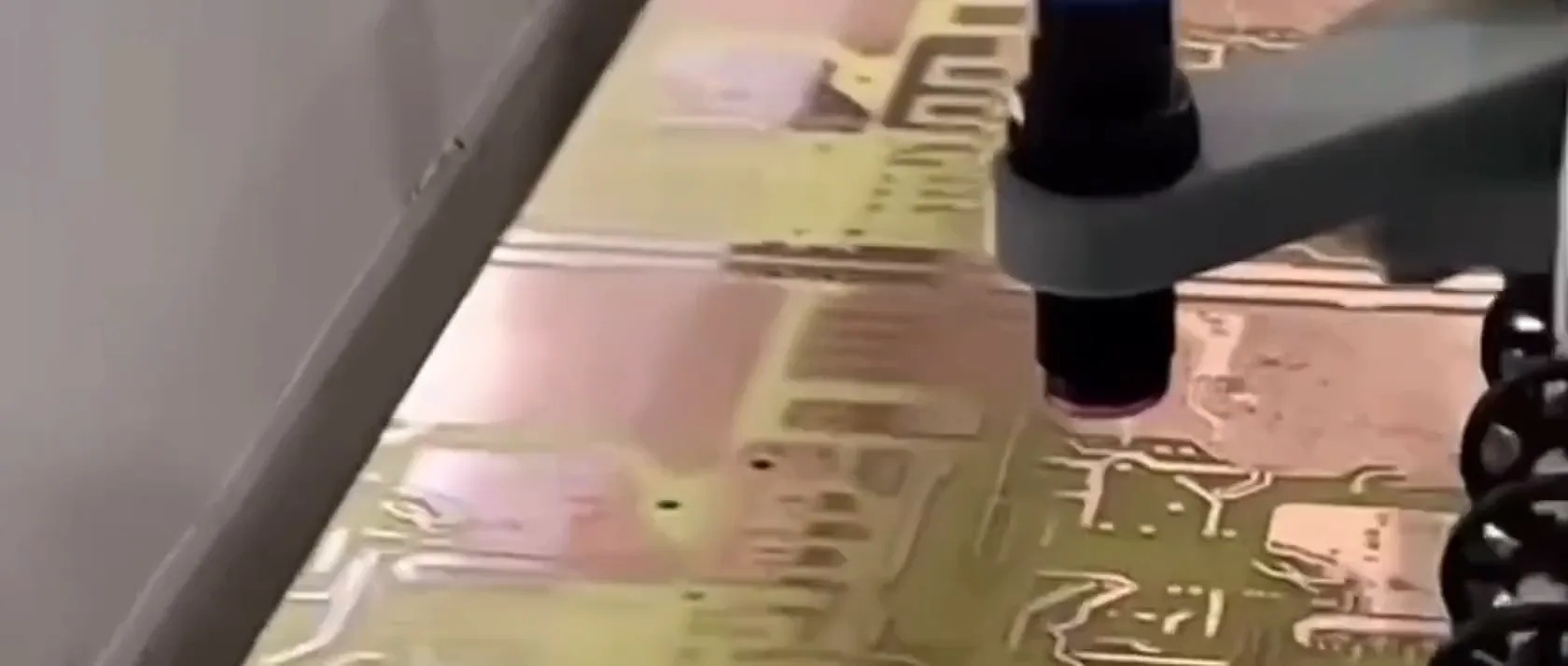
PCB manufacturing turns electronic design data (Gerber, ODB++ or IPC-2581) into physical printed circuit boards. Copper patterns are imaged and etched, layers are laminated, holes are drilled and plated, then solder mask, surface finish and electrical test are applied. Advanced boards repeat these steps with tighter tolerances and specialty materials.
A simple 2-layer board and a 30-layer HDI server board follow the same basic process chain. What separates them is how many times the steps repeat, how tightly registration and plating are controlled, and which laminates are used.
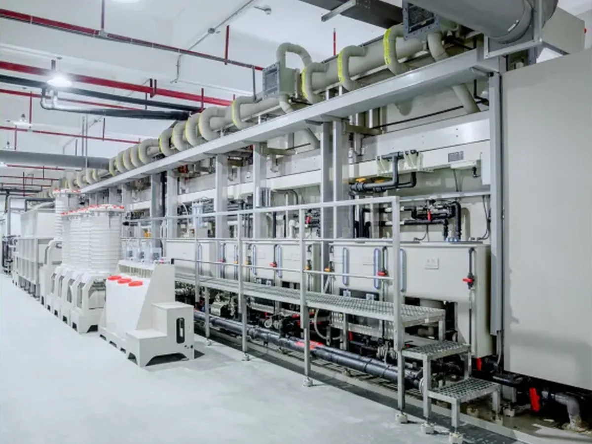
AstroPCB has focused on complex PCB manufacturing since 2008, through a managed network of 30+ partner factories and more than 1,000 engineers. Every order, prototype or production, starts with a written DFM review.
Board types
What we manufacture.
Multilayer PCB
Controlled-impedance stack-ups for digital, power and mixed-signal boards.
Multilayer PCBHigh frequency / RF PCB
Low-loss laminates for RF, microwave and mmWave.
High frequency PCBMetal core PCB
Copper-core and thermoelectric-separation boards for high-power LEDs and power electronics.
Metal core PCBThe PCB manufacturing process
Eight steps from data to board.
- Engineering & CAM: DFM review, stack-up confirmation, panelization.
- Inner-layer imaging and etching with direct laser imaging, then AOI of every inner layer.
- Lamination: cores and prepreg bonded under heat and pressure.
- Drilling: mechanical and laser drilling, including blind and buried vias.
- Plating: electroless then electrolytic copper in holes and on surfaces.
- Outer-layer imaging and etching.
- Solder mask, legend and surface finish (ENIG, HASL, OSP and more).
- Electrical test and final inspection, plus TDR impedance testing where specified.
HDI and blind/buried via designs repeat steps 3–5 for each sequential lamination. See blind & buried vias and microvias.

Capabilities
PCB manufacturing capabilities.
| Parameter | AstroPCB capability |
|---|---|
| Layer count | 1 to 30 layers |
| Board thickness | 0.2 to 6.0 mm |
| Copper weight | 0.5 to 10 oz |
| Min. line / space | 50 / 50 µm |
| Min. drill | 0.10 mm mechanical; 75 µm laser microvia |
| HDI | Up to 7-step sequential lamination, stacked or staggered microvias |
| Controlled impedance | ±8% with TDR verification |
| Special constructions | Rigid-flex, hybrid RF/digital, heavy copper, backdrilled vias, via-in-pad |
| Surface finishes | HASL, lead-free HASL, ENIG, ENEPIG, immersion silver, immersion tin, OSP, hard gold |
| Quality standard | IPC-6012 Class 2 by default, Class 3 on request |
Materials
Laminates for every performance target.
Megtron & Isola
Low-loss and high-reliability laminates for high-speed and high layer count.
Megtron materialsQuality
How quality is controlled.
- Written DFM review before every order
- AOI on inner and outer layers
- Electrical test: flying probe or fixture
- TDR impedance testing for controlled-impedance orders
- Microsection of plating and via quality
- IPC-6012 Class 2 / Class 3 acceptance; ISO 9001 quality system
- 99.6% on-time delivery across the factory network
Prototype to production
One process from 1 board to volume.
Prototypes are built with production materials and processes, so stack-ups and test results carry forward with no re-qualification. Start with a PCB prototype or a quick turn build, then scale on the same documentation. US teams can read PCB manufacturer for USA customers.
FAQ
PCB manufacturing questions, answered.
What is PCB manufacturing?
PCB manufacturing is the process of turning design data into printed circuit boards: imaging, etching, lamination, drilling, plating, solder mask, surface finish and electrical test.
How long does PCB manufacturing take?
Simple prototypes can be fabricated in 24–48 hours for eligible designs. Typical multilayer builds take 5–15 working days, and complex HDI or rigid-flex builds take longer, depending on lamination cycles.
What is the difference between PCB fabrication and PCB assembly?
Fabrication makes the bare board. Assembly solders components onto it. AstroPCB provides both; see PCB assembly.
What files are needed for PCB manufacturing?
Gerber RS-274X, ODB++ or IPC-2581 data, drill files and a fabrication drawing with stack-up, material, finish and tolerance requirements.
Which quality standard do you build to?
IPC-6012 Class 2 by default and Class 3 on request, under an ISO 9001 quality management system.
Do you manufacture small quantities?
Yes. Orders start from 1 piece and scale to production volumes.
Ready when your files are
Start PCB manufacturing with an engineering-reviewed quote.
Upload Gerber, ODB++ or IPC-2581 data. Every quote includes a written engineering DFM review, typically within one business day.