
AI server PCB · Data center
AI Server PCB & Data Center Board Manufacturing
20–30 layer boards on Megtron 7/8 with HDI, HVLP copper and back-drilling for 56G/112G PAM4 accelerator, GPU, switch and server designs, with power delivery for 300–700 W processors.
- Layers
- 20–30
- Laminates
- Megtron 7/8
- PAM4 lanes
- 112G
- Processor power
- 700 W

Overview
What an AI server PCB demands.
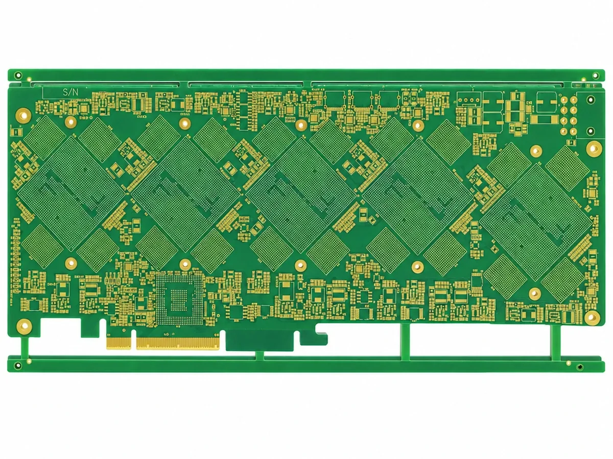
An AI server PCB is a high-layer-count board, typically 20–30 layers, built on ultra-low-loss laminate such as Megtron 7 or 8. It combines HDI breakout for 2,000–10,000-ball packages, controlled impedance for 56G/112G PAM4 SerDes and a power-delivery network for processors drawing 300–700 W.
AI accelerators, GPU modules, switch and server motherboards are among the most demanding boards in production. The laminate, copper foil, via structure and lamination sequence each consume part of a tight channel budget, and each one has to be co-designed with the power and thermal plan.
Signal integrity
Signal integrity at 56G and beyond.
AI accelerator interconnects run 56 Gbps PAM4 today, with 112G PAM4 in current designs and 224G on the roadmap. At these rates the laminate is the largest contributor to channel insertion loss. Standard FR-4 is unusable, Megtron 6 may be marginal on longer channels, Megtron 7 is the common baseline for 56G, and Megtron 8 or equivalent is specified for 112G and emerging 224G.
Copper roughness matters as much as laminate loss. HVLP (hyper very low profile) or RVLP copper on signal layers can reduce insertion loss by a meaningful fraction of a dB per inch at 28 GHz, the Nyquist frequency of 56G PAM4. That can decide whether a channel passes compliance.
| Data rate | Nyquist | Typical laminate | Copper |
|---|---|---|---|
| 25–28G NRZ | ≈ 14 GHz | Megtron 6 | VLP/HVLP |
| 56G PAM4 | ≈ 14 GHz | Megtron 6/7 | HVLP |
| 112G PAM4 | ≈ 28 GHz | Megtron 7/8 | HVLP |
| 224G PAM4 | ≈ 56 GHz | Next-gen ultra-low-loss | HVLP / smoothest available |
- Back-drilled via stubs on SerDes nets
- Spread or flat glass to limit fiber-weave skew
- TDR-verified impedance — controlled impedance
High layer count
High layer count construction.
AI server boards and switch boards commonly need 20 to 30 layers to carry hundreds of SerDes lanes, memory interfaces, power planes and I/O. Sequential lamination with blind and buried vias connects signal layers without spending routing space on through-holes. Laser microvias, stacked vias and via-in-pad allow escape from fine-pitch BGAs with thousands of balls.
Thick boards (often 3–6 mm) need tight registration, controlled resin flow and warpage management across very large panels. Server motherboards can exceed 500 × 500 mm. See multilayer PCB and HDI PCB.
Power delivery
Power delivery for 300–700 W processors.
A modern accelerator can draw 300–700 W at sub-1 V core rails, which means hundreds of amps. Getting that from the VRMs to the package needs heavy copper planes (2–4 oz on power layers), low-impedance PDN design and dense via arrays at the package. Power-plane design also changes stack-up geometry and impedance on adjacent signal layers, so SI and PI must be co-designed during stack-up planning.
- 2–4 oz power and ground planes — heavy copper
- Dense power via arrays and via-in-pad at the package
- IR-drop and PDN impedance analysis on the real layout
Thermal
Thermal management.
With hundreds of watts concentrated in a small area, thermal design is part of the PCB. Thermal-via arrays under high-power devices move heat into internal planes, which spread it toward heat sinks, cold plates or liquid-cooling interfaces. Via pattern, plane coverage and the board-to-heatsink interface all set junction-to-ambient thermal resistance, and thick boards with many planes need extra care in lamination to avoid resin starvation.
Board types
AI and data center board types.
Capabilities
AI and data center PCB capabilities.
| Parameter | Capability |
|---|---|
| Layers | 20–30 |
| Laminates | Megtron 6/7/8, Tachyon-class |
| HDI | Up to 7-step, stacked copper-filled microvias |
| Impedance | ±8% standard; tighter reviewed |
| Vias | Back-drill, via-in-pad, blind/buried |
| Thickness | Up to about 6.0 mm |
| Copper | HVLP signal foil; 2–4 oz power planes |
Case framework
How we approach an accelerator build.
Our AI accelerator HDI framework shows how stacked-microvia breakout, lamination count, laminate selection and power delivery are traded off to keep a 30-layer board buildable and cost-controlled.
Design for manufacture
Design choices that control cost and yield.
Most cost on an AI board comes from lamination cycles, board thickness and drilled-hole count. Each extra sequential lamination adds material, press time and yield risk. Staggered microvias are often cheaper and more robust than three-level stacks, and limiting the number of distinct blind-via spans keeps the build sequence short.
Thick boards with tiny holes push aspect ratio. Keep through-hole aspect ratio within the fabricator’s published limit, use back-drilling instead of extra thickness to manage stubs, and balance copper across the stack so a 4–6 mm board stays flat through multiple reflows and press-fit connector insertion.
- Prefer 2-level stacked or staggered microvias where breakout allows
- Minimize distinct blind/buried spans
- Hold through-hole aspect ratio within published limits
- Balance copper to control warp on thick boards
- Specify back-drill depth and keep-out per net
RFQ
What to send for an AI server PCB quote.
- Layer count, thickness and target stack-up
- Laminate grade (Megtron 6/7/8) and copper profile
- Impedance targets and channel loss budget
- HDI structure and via-in-pad locations
- Back-drill nets and depth
- Power rails, current and copper weights
FAQ
Frequently asked questions.
What PCB technology do AI accelerators require?
HDI with 20–30 layers, fine-pitch BGA breakout (0.4–0.65 mm), ultra-low-loss laminates for 56–112G SerDes, heavy-copper power planes and back-drilling.
What material is used for AI server PCBs?
Megtron 7 for most 56G designs and Megtron 8 or Tachyon-class laminates for 112G/224G.
How many layers do AI server boards have?
Typically 20–30, depending on BGA size, SerDes count and power rails.
Why does copper roughness matter?
At 28 GHz and above, skin effect concentrates current at the copper surface, so rough foil adds loss. HVLP foil reduces it.
Do you back-drill?
Yes, via stubs on high-speed nets are back-drilled to a specified depth.
Can you build large server boards?
Yes; large panels need enhanced registration and warpage control, which we review during DFM.
Ready when your files are
Send your design and compliance requirements.
Upload Gerber, ODB++ or IPC-2581 data. Every quote includes a written engineering DFM review, typically within one business day.