
BMS PCB · Power electronics
BMS PCB & Power Electronics PCB Manufacturing
Heavy copper, metal core and high-voltage isolation for battery management systems, inverters, motor drives, DC-DC converters, chargers and power supplies.
- Copper per layer
- 2–10 oz
- Isolation designs
- 500 V+
- Metal core options
- IMS
- Automotive-grade
- EV

Overview
Power electronics PCBs, explained.
Power electronics PCBs carry high currents, dissipate concentrated heat and isolate high voltages from low-voltage control. A BMS PCB (battery management system board) monitors each cell, balances charge, switches pack current and reports state of charge and health, putting precision analog, isolation and power switching on one board.
BMS boards, motor drives, inverters, DC-DC converters, power supplies and chargers share four board-level problems: current capacity, heat removal, isolation and mechanical robustness in vibrating environments such as EVs and industrial equipment. Each one is solved partly in the layout and partly in the fabrication process.
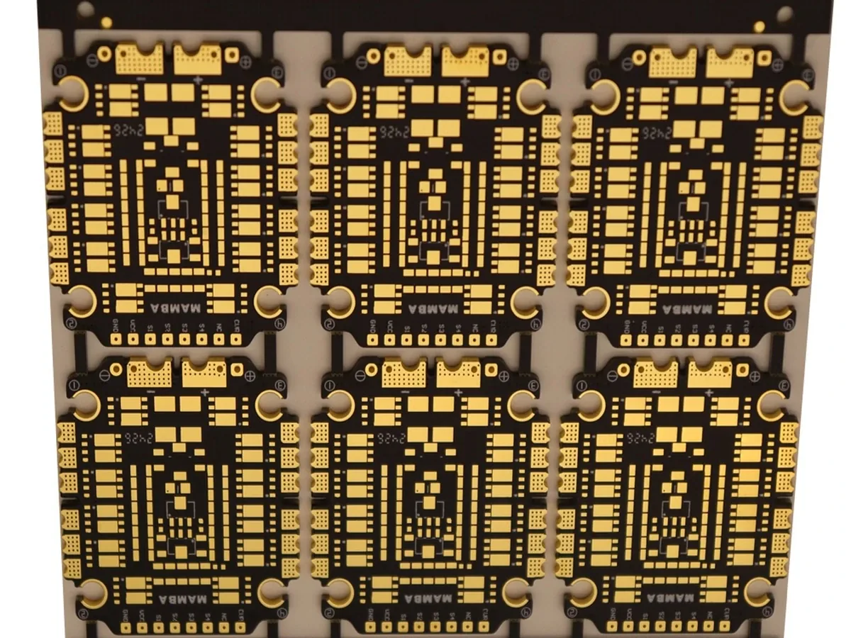
BMS PCB requirements
BMS PCB requirements.
A BMS PCB measures individual cell voltages, often to millivolt accuracy, while those cells sit hundreds of volts above system ground. It must isolate the cell-monitoring front end from the communication interface (often 500 V+ isolation), combine precision analog measurement with digital communications, and dissipate heat from balancing resistors and MOSFETs during active balancing.
EV BMS boards also meet automotive reliability requirements: -40 °C to +125 °C cycling, vibration endurance and lifetimes beyond 10 years. Heavy copper (2–4 oz) on power layers, high-Tg laminates such as Isola 370HR and automotive-grade finishes are standard. See also battery management system PCB design.
- Cell-sense routing kept away from switching nodes
- Isolation slots and keep-outs under isolators
- Thermal relief for balancing resistors
- Conformal coating for high-voltage reliability
Heavy copper
Heavy copper for power distribution.
Boards carrying 10, 20 or 50+ A cannot use 1 oz traces. The width needed would consume the board. Heavy copper from 2 oz to 10 oz gives practical trace widths for these currents. As a rule of thumb, a 100 mil trace in 4 oz copper carries roughly 12 A at a 20 °C rise, while 1 oz copper would need a trace about four times as wide or a bus bar.
Heavy power layers can sit next to standard-weight signal layers in one board. A typical stack-up might use 3 oz on two power layers and 1 oz on signal and control layers, with etch and plating parameters set per layer.
| Copper weight | Thickness | Typical min. trace / space |
|---|---|---|
| 2 oz | 70 µm | ≈ 125 / 125 µm |
| 3 oz | 105 µm | ≈ 150 / 150 µm |
| 4 oz | 140 µm | ≈ 200 / 200 µm |
| 6 oz | 210 µm | ≈ 250 / 250 µm |
| 10 oz | 350 µm | ≈ 380 / 380 µm |
Thermal management
Thermal management in power PCBs.
Heat concentrates at switching devices, current-sense resistors, inductor pads and connectors. The PCB must move it away before junctions exceed safe limits. The main tools are thermal-via arrays under hot components connected to internal planes, heavy copper planes acting as heat spreaders, and copper-core metal substrates for single-layer power circuits that need the best possible thermal conductivity. For extreme heat flux, embedded copper coins are an option.
Thermal vias
Arrays under MOSFETs and shunts into internal planes.
High-voltage isolation
High-voltage isolation.
High voltages often share the board with low-voltage control. Creepage and clearance between them must meet the applicable standard: IPC-2221 for general design, IEC 62368-1 for IT and AV equipment, IEC 60601-1 for medical devices, and IEC 60664 / UL 840 for insulation coordination. These distances drive trace spacing, slot placement, outline geometry and component placement.
The fabricator must preserve them in production. Solder mask slivers, copper residue and rough board edges can all reduce effective isolation. We verify slot geometry, edge quality and spacing in DFM, and hi-pot testing is available on request.
Applications
Power electronics applications.
| Application | Key board features |
|---|---|
| EV BMS / ESS BMS | Isolation, precision sense, 2–4 oz power |
| Traction inverter / gate drivers | Heavy copper, low-inductance loops, isolation |
| On-board chargers / DC-DC | Heavy copper, magnetics pads, thermal vias |
| Motor drives | Heavy copper, metal core options |
| Industrial power supplies | Creepage per IEC 62368-1, high-CTI laminate |
| Solar / storage inverters | High voltage, outdoor reliability |
Typical stack-up
Example 6-layer power stack-up.
| Layer | Use | Copper |
|---|---|---|
| L1 | Components, signal | 1–2 oz |
| L2 | Ground | 2 oz |
| L3 | Power | 3–4 oz |
| L4 | Power | 3–4 oz |
| L5 | Ground | 2 oz |
| L6 | Components, signal | 1–2 oz |
Design rules
Layout rules for power boards.
Keep high-di/dt switching loops as small as possible: place input capacitors, switches and return paths tightly, using adjacent layers for the loop. Use Kelvin connections on current-sense resistors so measurement traces do not carry load current. Spread heavy current across several vias, since each via has its own current limit, and use copper pours rather than single wide traces where the board allows.
Give magnetics and high-voltage nodes generous clearance, slot the board under isolators where creepage is tight, and keep the high-voltage area free of silkscreen and solder-mask slivers that could trap contamination.
- Minimize switching loop area
- Kelvin-connect current shunts
- Use multiple vias for high-current transitions
- Slot under isolators when creepage is tight
- Specify hi-pot test voltage on the drawing
RFQ
What to send for a power PCB quote.
- Copper weight per layer and maximum currents
- System voltage and isolation standard
- Thermal requirements and heatsink interface
- Operating environment (automotive, industrial, outdoor)
- Hi-pot and test requirements
- Assembly needs: see PCB assembly
FAQ
Frequently asked questions.
What is a BMS PCB?
The circuit board of a battery management system: it monitors cells, balances charge, controls current and protects the pack.
What current can PCB traces handle?
It depends on copper weight, width and allowed temperature rise. A 10 mil 1 oz external trace carries about 1 A at 10 °C rise; a 100 mil 4 oz trace carries roughly 12–15 A.
How much copper does a power PCB need?
Often 2–4 oz on power layers, up to 10 oz for very high current; size traces with the trace width calculator.
How do you manage heat in power PCBs?
Heavy copper, thermal-via arrays, copper-core substrates and, for extreme cases, embedded copper coins.
How do you achieve high-voltage isolation?
Creepage and clearance to the applicable standard, routed slots, high-CTI laminates, clean edges and hi-pot testing.
Which safety standards apply?
IPC-2221 for spacing, UL 796 for listed boards, IEC 62368-1 for IT/AV power supplies, IEC 60601-1 for medical and IEC 60664 / UL 840 for insulation coordination.
Ready when your files are
Send your design and compliance requirements.
Upload Gerber, ODB++ or IPC-2581 data. Every quote includes a written engineering DFM review, typically within one business day.