
SMT assembly services · Surface mount PCBA
SMT Assembly Services: 01005 Passives to 0.3 mm BGAs
Automated surface-mount assembly with solder paste inspection, vision placement, profiled reflow, AOI and X-ray, from prototype to production volumes.
- Smallest passive
- 01005
- BGA pitch
- 0.3 mm
- Placement accuracy
- ±25 µm
- First-pass yield
- >99.5%

What is SMT assembly
Surface mount assembly, explained.
SMT (surface mount technology) assembly solders components directly onto pads on the PCB surface, with no drilled holes. It allows smaller parts, higher density, faster automated placement and lower assembly cost than through-hole. The process is paste printing, placement, reflow and inspection.
AstroPCB SMT assembly services handle everything from 01005 passives (0.4 × 0.2 mm) to 0.3 mm pitch BGAs, on boards we fabricate ourselves, so pad finish, via-in-pad and stencil design are aligned.
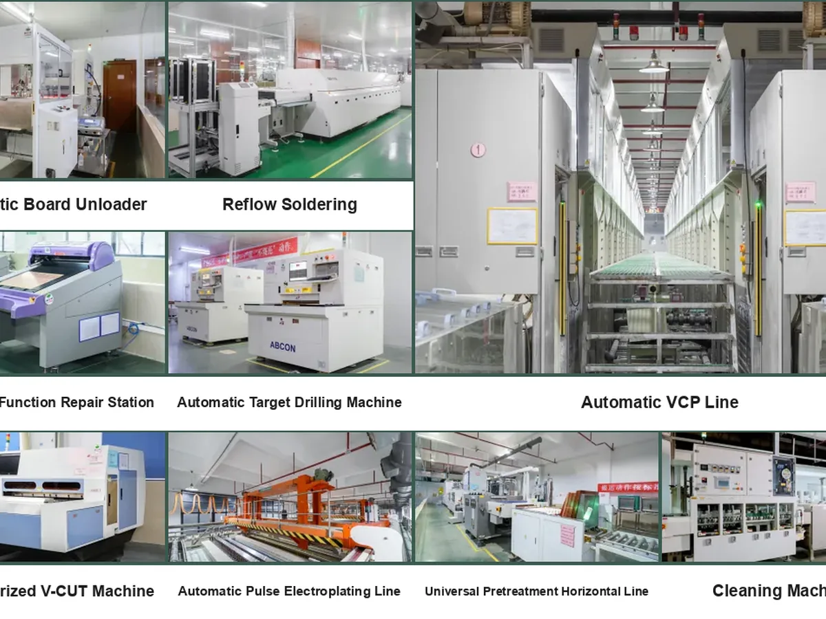
SMT capabilities
SMT assembly capabilities.
| Parameter | Capability |
|---|---|
| Smallest passive | 01005 (0.4 × 0.2 mm) |
| Fine-pitch packages | BGA, CSP, QFN, LGA, PoP down to 0.3 mm pitch |
| Placement accuracy | ±25–50 µm with vision alignment |
| Placement rate | 20,000–60,000 components per hour per line |
| Stencil | Laser-cut stainless, 100–150 µm typical; step stencils |
| Inspection | SPI, AOI, X-ray, first-article inspection |
| Yield | First-pass yield above 99.5% |
| Sides | Single- and double-sided SMT; mixed technology with THT |
Process
The SMT process step by step.
Paste print + SPI
Stencil prints paste; SPI measures volume, height and offset on every pad.
Placement
Vision-checked pick-and-place verifies orientation and polarity.
Reflow
Preheat, soak, reflow and cooling profiled for alloy and thermal mass.
AOI + X-ray
Bridging, tombstoning and hidden BGA/QFN joints inspected.
Fine pitch
Fine-pitch and advanced packages.
0.3–0.4 mm BGAs, QFNs with thermal pads, CSP, PoP and 01005 passives need thinner stencils, smaller apertures, tighter placement and mandatory X-ray. We review pad geometry, finish and via-in-pad before assembly.
For the board side, see via in pad, HDI PCB and ENIG surface finish.

Double-sided SMT
Double-sided SMT boards.
Double-sided boards are assembled in two passes. The reflow profile and component placement are planned so that first-side joints survive the second reflow, and heavy parts are kept on the second side or glued where necessary.
Process detail
Inside each SMT step.
Paste printing uses a laser-cut stainless stencil, typically 100–150 µm thick, aligned to the board. Aperture design controls paste volume on each pad. Solder paste inspection measures volume, height and offset on every pad before placement, catching print defects at the cheapest point to fix them.
Pick-and-place machines take parts from reels, trays and tubes and place them with ±25–50 µm accuracy at 20,000–60,000 components per hour, with vision checking orientation and polarity. Reflow follows a profile of preheat, soak, reflow peak and controlled cooling set for the alloy, component thermal mass and board construction.
Design for assembly
Design-for-assembly tips for SMT.
- Use IPC-7351 land patterns for every footprint
- Provide 3 global fiducials plus local fiducials near fine-pitch parts
- Keep components ≥ 3 mm from conveyor edges or add rails
- Use via-in-pad (filled and capped) rather than open vias in pads — via in pad
- Orient polarized parts consistently
- Specify ENIG or ENEPIG for fine pitch
Quality
SMT quality metrics.
- First-pass yield above 99.5%
- Defect rate under 50 DPMO
- IPC-A-610 Class 2 by default, Class 3 on request
- First-article inspection per new design
- Traceability records on request
FAQ
SMT assembly questions.
What is the smallest SMT component you can place?
01005 passives (0.4 × 0.2 mm), and fine-pitch QFP/BGA packages down to 0.3 mm pitch at ±25 µm placement accuracy.
What is your SMT defect rate?
First-pass yield above 99.5% with a defect rate under 50 DPMO, supported by SPI, AOI and X-ray.
Do you X-ray BGAs?
Yes. X-ray is used for BGA, QFN, LGA and other bottom-terminated packages.
Can you assemble double-sided SMT boards?
Yes, in two reflow passes with profiles planned to protect first-side joints.
Do you also do through-hole?
Yes. Mixed-technology boards combine SMT with through-hole and selective or wave soldering. See PCB assembly.
What files are needed?
Gerbers, BOM with manufacturer part numbers and a centroid file, plus quantity and sourcing preference.
What stencil thickness do you use?
Typically 100–150 µm laser-cut stainless, with step stencils where fine-pitch and large parts share a board.
Ready when your files are
Upload BOM and centroid for an SMT quote.
Upload Gerber, ODB++ or IPC-2581 data. Every quote includes a written engineering DFM review, typically within one business day.