
HDI PCB manufacturer · High density interconnect
HDI PCB Manufacturer for High Density Interconnect Boards
Laser microvias, via-in-pad and up to 7-step sequential lamination for fine-pitch BGAs and compact, high-speed designs, with each stack-up checked by an engineer before it goes to production.
- Sequential lamination (up to 7+N+7)
- 7-step
- Laser-drilled microvia
- 75 µm
- Min. line / space
- 50 µm
- Impedance tolerance
- ±8%
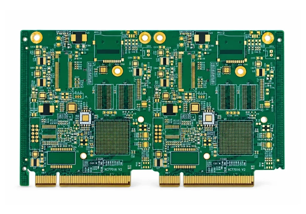
What is an HDI PCB
High density interconnect, explained.
An HDI PCB (high density interconnect printed circuit board) uses laser-drilled microvias, blind and buried vias, via-in-pad and finer line/space to route more connections per square inch than a conventional through-hole multilayer board. Designers choose HDI circuit boards for fine-pitch BGAs, smaller form factors and short, low-inductance interconnects for high-speed signals.
A standard multilayer board connects layers with mechanically drilled through-holes that consume routing space on every layer. HDI builds the board in sequential stages. Thin dielectric layers are laminated onto a core and connected with microvias only where they are needed, which frees routing channels under dense components.
As an HDI PCB manufacturer, AstroPCB works from the routing problem, not a catalogue. We recommend the smallest number of build-up steps, via types and lamination cycles that still escapes your BGA and meets your impedance and reliability targets, because each extra cycle adds cost, lead time and yield risk.
- Fine-pitch BGA escape at 0.65 mm, 0.5 mm and 0.4 mm pitch
- Smaller, lighter boards with fewer layers than an equivalent through-hole design
- Shorter via stubs and better signal integrity for high-speed channels
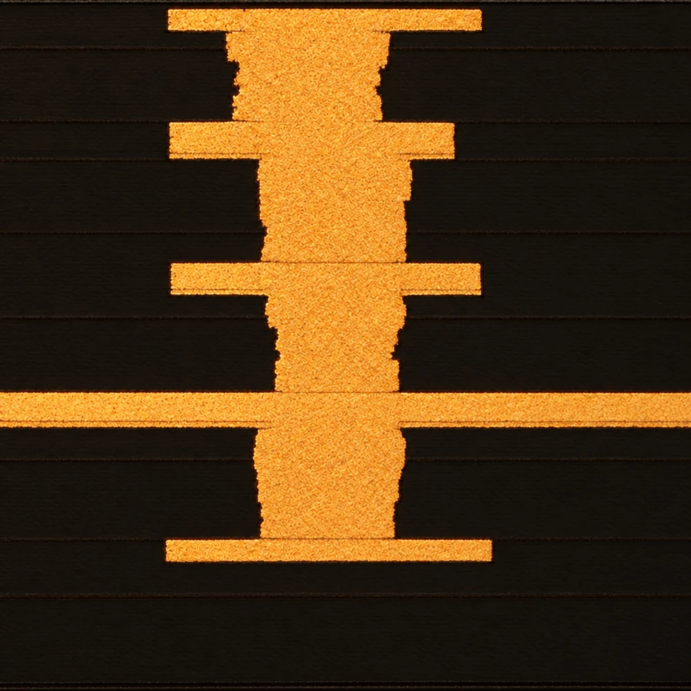
Microsection of a sequential-lamination HDI build-up.
Why AstroPCB
Why engineers choose AstroPCB as their HDI PCB manufacturer.
Choosing an HDI PCB manufacturer comes down to whether the build-up will survive lamination, assembly and field use. Our engineers review every set of HDI circuit boards against the stack-up, via schedule and reliability target before quoting, so you get a buildable plan rather than a capability list.
- HDI from 1+N+1 to 7+N+7 with stacked or staggered microvias and copper-filled via-in-pad
- Microsection and TDR verification on HDI coupons
- Engineering since 2008: 1,000+ engineers and 30+ partner factories in Shenzhen, Xi’an, Chengdu and Hangzhou
- Written DFM review on every order, prototype or production, before fabrication starts
- 99.6% on-time delivery across the partner factory network
- From 1 piece to volume with the same stack-up and process controls
- IPC Class 2 by default, Class 3 on request, with inspection records and batch traceability
- Fabrication plus assembly: component sourcing, SMT and tracked worldwide shipping
HDI PCB capabilities
HDI circuit boards: manufacturing capabilities.
Use these figures for early stack-up planning. If your design sits close to one of these limits, flag it in the RFQ so our engineers review it first.
| Parameter | AstroPCB capability |
|---|---|
| HDI structures | 1+N+1, 2+N+2, 3+N+3 up to 7+N+7 (7-step sequential lamination); any-layer HDI reviewed per design |
| Layer count | 4 to 30 layers |
| Laser microvia diameter | 75 µm minimum laser drill |
| Microvia aspect ratio | Up to 1:1 |
| Microvia structures | Stacked or staggered; copper-filled microvias for stacked and via-in-pad designs |
| Via-in-pad | Epoxy-filled and copper-capped (VIPPO) for BGA and fine-pitch pads |
| Min. line / space | 50 / 50 µm |
| Min. mechanical drill | 0.10 mm |
| Layer-to-layer registration | ±2 mil (50 µm) for HDI constructions |
| Controlled impedance | ±8% with confirmed stack-up and TDR coupon verification |
| Surface finishes | ENIG, ENEPIG, immersion silver, immersion tin, OSP, hard gold, HASL / lead-free HASL |
| Acceptance standard | IPC-6012 Class 2 by default, Class 3 on request |
HDI stack-up structures
Choose the simplest HDI build that routes.
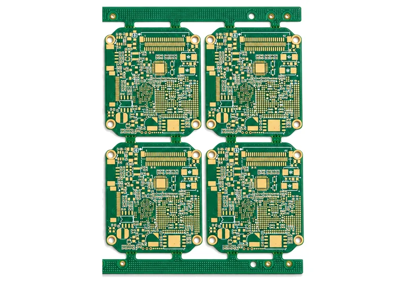
1+N+1 HDI
One microvia build-up layer on each side of a laminated core, combined with through vias and, optionally, buried vias. It is the most cost-efficient HDI structure and often enough to escape a 0.65–0.8 mm pitch BGA.
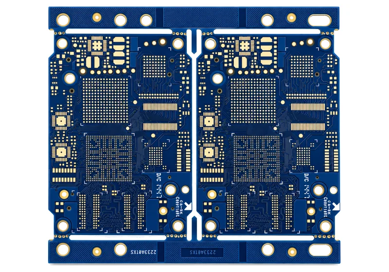
2+N+2 and 3+N+3 HDI
Two or more sequential build-up layers per side, with stacked or staggered microvias. This is the usual choice for 0.5 mm and 0.4 mm pitch processors, FPGAs and dense SiP or RF front-end modules.
Any-layer HDI
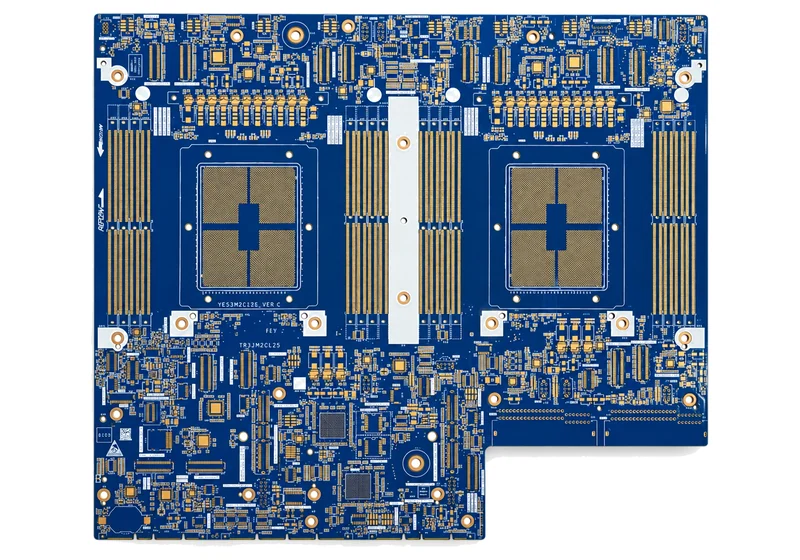
Every layer is interconnected by copper-filled, stacked microvias, so any layer can reach any adjacent layer. It gives the highest routing density, used in smartphones, wearables and AI accelerator modules, and needs the most careful reliability review.
HDI PCB design guidelines
Design decisions that make HDI buildable.
Most HDI cost and yield problems are decided at layout. The following points are the ones our DFM reviews raise most often.
| BGA pitch | Typical escape strategy |
|---|---|
| 1.0 mm / 0.8 mm | Dog-bone fan-out with through vias; HDI only if layer count or board size must shrink |
| 0.65 mm | 1+N+1 microvias or via-in-pad on inner rows |
| 0.5 mm | Via-in-pad with 1+N+1 or 2+N+2, depending on ball count |
| 0.4 mm and below | 2+N+2 or higher, stacked or staggered microvias, copper-filled via-in-pad |
- Staggered vs stacked microvias: staggered microvias are generally more robust in thermal cycling. Stacks of more than two levels need copper fill and a deliberate reliability review.
- Keep microvia aspect ratio ≤ 1:1: the dielectric thickness of each build-up layer must suit the laser via diameter so plating stays reliable.
- Mark every via-in-pad location: filled and capped pads add process steps. Call them out explicitly in the drill table and fabrication drawing.
- Balance copper and keep the build symmetric: asymmetric build-ups warp during repeated lamination and reflow.
- Define impedance per layer: thin build-up dielectrics change trace geometry. Send target impedance and reference planes with the stack-up. See our impedance calculator.
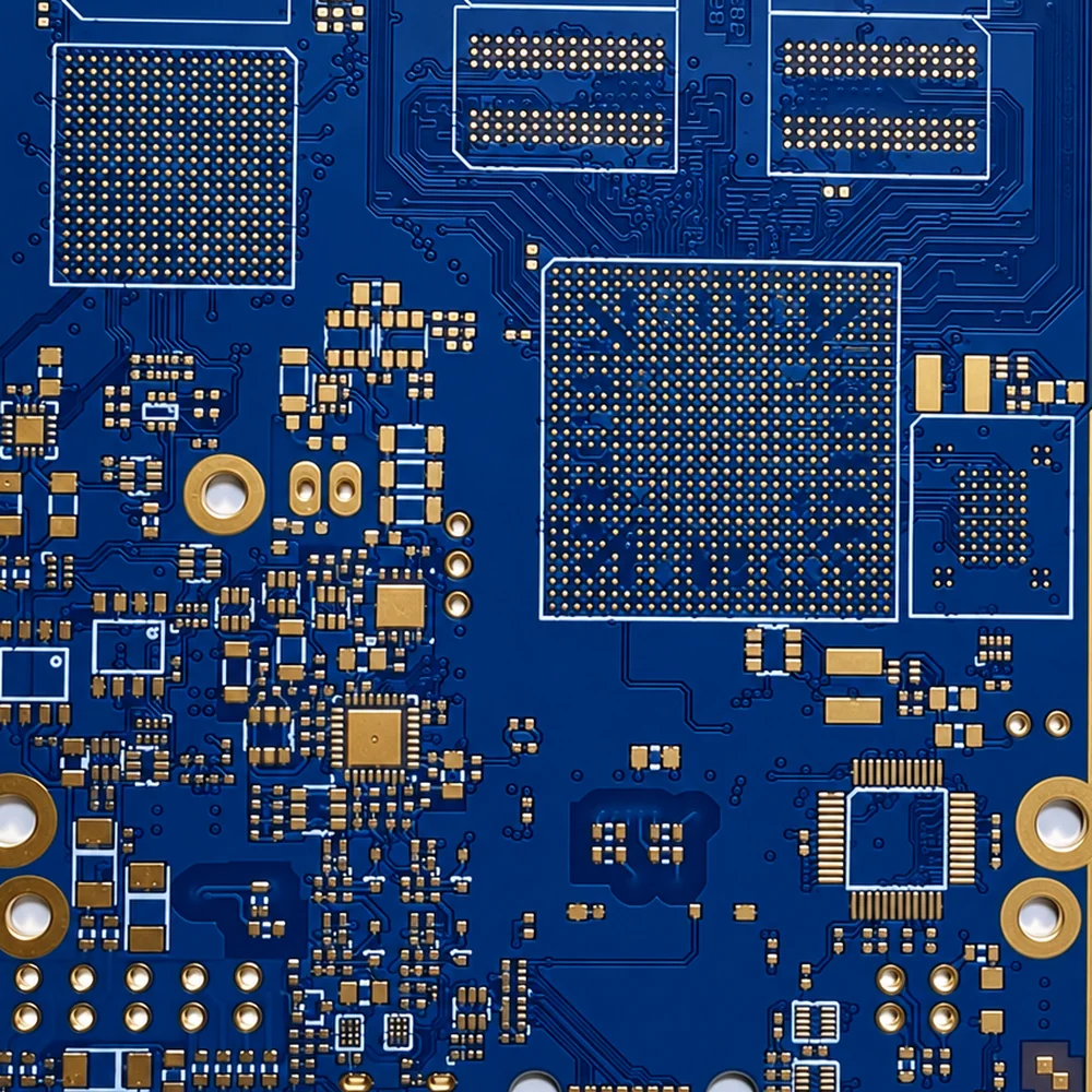
Via-in-pad escape under a fine-pitch BGA.
HDI materials
Laminates matched to signal speed and lamination count.
High-Tg FR-4
High-Tg FR-4 systems with laser-drillable prepregs suit most consumer, industrial and IoT HDI boards, and they hold up through several lamination cycles.
FR-4 material guideLow-loss: Megtron 6 / 7
For PCIe, 56G/112G SerDes and AI accelerator boards that need low Df across many build-up layers.
Megtron materialsIsola 370HR & hybrids
A robust choice for repeated lamination. Hybrid builds can add Rogers layers for RF sections.
Isola 370HRWhere HDI is used
Industries that depend on HDI PCBs.

AI & data center
Accelerator modules, switch and server boards with large BGAs, high layer counts and low-loss HDI build-ups.
AI & data center PCB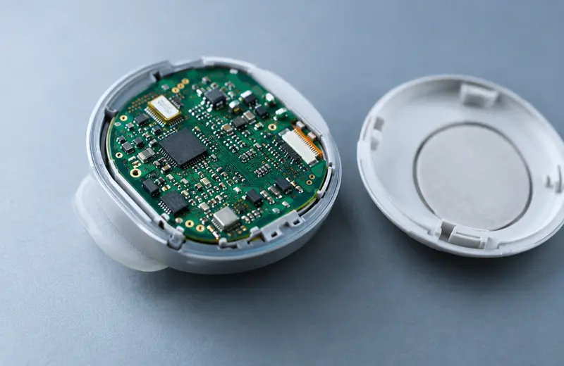
Medical & wearables
Miniaturized monitoring, imaging and handheld devices where board area and reliability both matter.
Medical PCB
Automotive & aerospace
ADAS, radar and avionics modules that combine HDI density with IPC Class 3 reliability requirements.
Automotive PCBQuality & verification
How every HDI build is checked.

HDI failures hide inside the board, at the microvia-to-target-pad interface, in plating voids or in misregistered build-up layers. Our verification plan is built around those risks.
- Written DFM review of stack-up, via schedule and lamination sequence before release
- AOI on inner and build-up layers
- Microsection analysis of microvia plating and fill on coupons
- TDR impedance testing on controlled-impedance coupons
- 100% electrical test (flying probe or fixture)
- IPC-6012 Class 2 or Class 3 acceptance, with inspection records on request
HDI PCB cost
What drives HDI PCB cost.
An HDI board costs more than a through-hole multilayer of the same size, but a well-planned HDI design often uses fewer layers or a smaller outline, which narrows the gap. These factors move the price most:
- Number of lamination cycles: each additional build-up step is a full press, drill and plating cycle
- Stacked, copper-filled microvias versus staggered microvias
- Via-in-pad fill-and-cap area and count
- Laminate system: FR-4 vs low-loss materials
- Total layer count and finished thickness
- Line/space and drill sizes close to the published limits
- Quantity and panel utilization
- Class 3 inspection and documentation requirements
Upload your design for a firm price. Our quote shows which choices drive cost and where a simpler build-up would still work.
Request an HDI quote
What to include in your HDI RFQ.
- Gerber, ODB++ or IPC-2581 data plus fabrication drawing
- Target stack-up, HDI structure (e.g. 2+N+2) and finished thickness
- Via schedule: microvia, blind, buried and through-via start/stop layers
- Via-in-pad locations and fill/cap requirements
- Impedance table with layers and reference planes
- Material preference and whether substitutes are allowed
- IPC class, surface finish and test requirements
- Quantities: prototype and expected production volume
FAQ
HDI PCB questions engineers ask us.
What is an HDI PCB?
An HDI (high density interconnect) PCB uses laser-drilled microvias, blind and buried vias, via-in-pad and fine line/space to achieve higher wiring density than a conventional multilayer board. It is built by sequential lamination, adding thin build-up layers to a core in stages.
What is the difference between HDI and a standard multilayer PCB?
A standard multilayer PCB connects layers mainly with mechanically drilled through-holes. HDI adds laser microvias that connect only adjacent layers, so routing space on other layers stays free. That gives more connections per unit area, fine-pitch BGA escape and often fewer total layers.
Which HDI structures does AstroPCB manufacture?
AstroPCB builds HDI from 1+N+1 up to 7+N+7 (7-step sequential lamination) with stacked or staggered microvias, and reviews any-layer HDI designs case by case. HDI boards range from 4 to 30 layers.
What is the smallest microvia you can drill?
Our minimum laser-drilled microvia is 75 µm with an aspect ratio up to 1:1; the minimum mechanical drill is 0.10 mm.
When does a design need HDI?
HDI is usually needed when BGA pitch is 0.65 mm or finer, when the board must shrink, or when through-hole vias leave too few routing channels or too much stub length for high-speed signals. At 0.8 mm pitch and above, a through-hole design is often still possible.
Are stacked or staggered microvias better?
Staggered microvias are generally more robust in thermal cycling and cheaper. Stacked, copper-filled microvias save space and are needed in very dense layouts, but stacks of more than two levels need a careful reliability review. We recommend a structure during DFM.
How much does an HDI PCB cost?
Cost depends mainly on the number of lamination cycles, microvia structure, via-in-pad count, material, layer count and quantity. Upload your files for an engineering-reviewed quote, typically within one business day.
Do you offer HDI PCB assembly?
Yes. AstroPCB provides component sourcing and SMT assembly for HDI boards, including fine-pitch BGAs. See PCB assembly services.
Ready when your files are
Send your HDI stack-up for an engineering-reviewed quote.
Upload Gerber, ODB++ or IPC-2581 data. Every quote includes a written engineering DFM review, typically within one business day.