
Engineering scenarios
PCB Case Studies: How We Approach Complex Builds
Production HDI builds from AstroPCB, with stack-ups, materials and process controls (customer names withheld under NDA), plus engineering scenarios showing how our DFM review handles HDI, rigid-flex, radar and heavy-copper boards.
- Production case studies
- 5
- Layer range
- 12–26
- Laser via cycles
- 2–12
- Laminates
- TU-933+ · M6

Production builds
Production HDI case studies.
AstroPCB case studies document real production boards: layer count, HDI structure, laminate, copper and the manufacturing controls that made each build work. Customer names are withheld under NDA; every technical value comes from the production stack-up and project sheet.

Any-Layer HDI PCB: 26 Layers, 12 Laser Cycles on TU-933+
26 layers on TU-933+, 12 laser drill and copper-fill cycles, 0.1 mm thin cores and ≤25 µm fill flatness for a 5G product.
Read the case study400G Optical Module PCB: 12-Layer 4-Step HDI with Segmented Gold Fingers
12-layer 4-step stacked HDI on TU-933+, 4-level 8-segment gold fingers, ±6% impedance and ±0.1 mm thickness tolerance.
Read the case study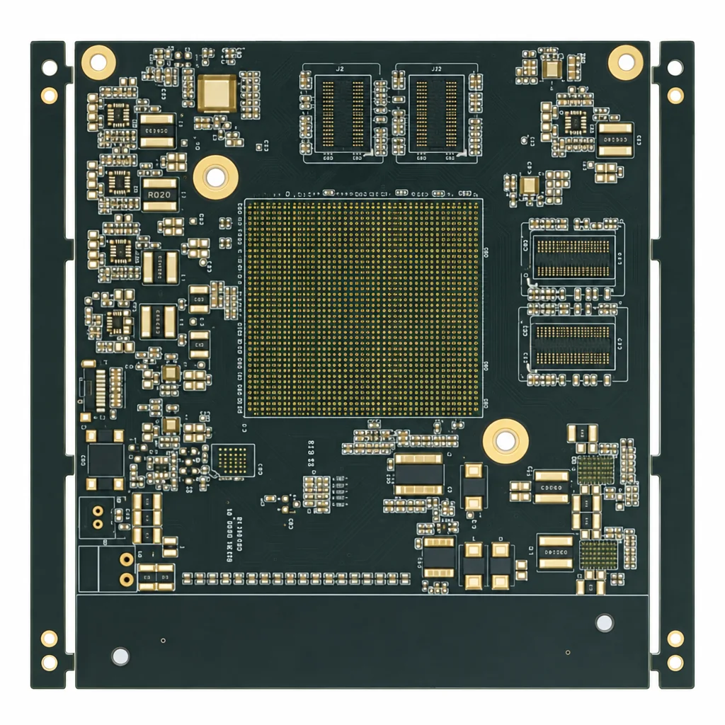
Automotive HDI PCB: 16-Layer 4-Step Stacked Microvias on Megtron 6
16-layer 4-step stacked microvias on Megtron 6, 6.5 mil hole-to-copper and zero open repair for a vehicle control unit.
Read the case study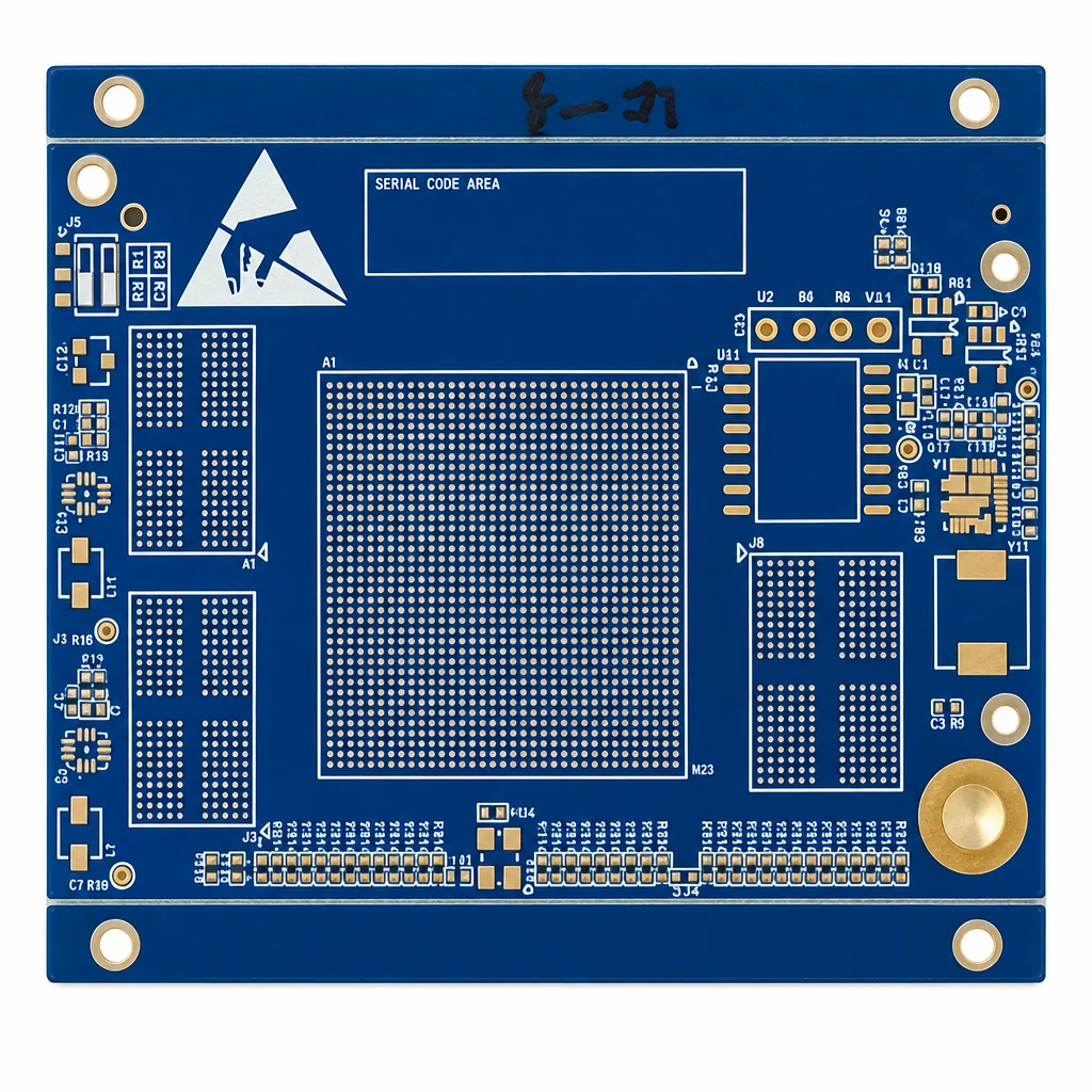
Asymmetric HDI PCB: 14-Layer 2-Step Stacked Vias on Megtron 6
14 layers on Megtron 6, L2 stacked laser vias plus several blind via spans, 6 mil hole-to-copper, all-microvia outer layers.
Read the case study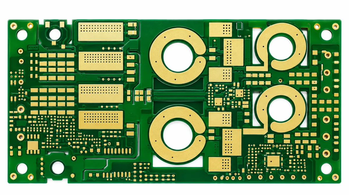
Heavy Copper HDI PCB: 12-Layer 3 oz High-Tg Board with Crossed Blind & Buried Vias
12-layer high-Tg FR-4, 3 oz inner copper, laser vias through multiple prepreg plies and crossed blind/buried vias.
Read the case study| Case study | Layers | Structure | Laminate | Application |
|---|---|---|---|---|
| 26-layer any-layer HDI | 26 | Any-layer, 12 laser cycles | TU-933+ | 5G sensing & control |
| 400G optical module PCB | 12 | 4-step stacked HDI, segmented gold fingers | TU-933+ | Data center optics |
| 16-layer automotive HDI | 16 | 4-step stacked (4+8+4) | Megtron 6 | Vehicle control unit |
| 14-layer asymmetric HDI | 14 | Asymmetric 2-step stacked | Megtron 6 | Broadcast control system |
| Heavy copper HDI battery board | 12 | 3 oz inner, crossed blind/buried | High-Tg FR-4 | Automotive battery |
Scenarios
Engineering scenarios.

AI accelerator HDI
Stacked microvias for 0.5 mm BGA escape with 56G impedance; reducing lamination cycles through stack-up optimization.
Read the framework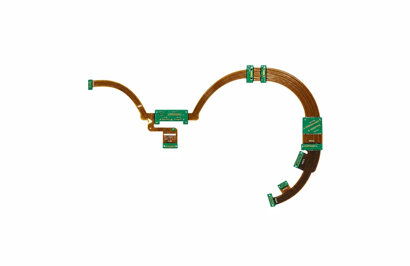
Medical rigid-flex
Multi-section rigid-flex with impedance through flex zones, dynamic flex endurance and Class 3 traceability.
Rigid-flex PCB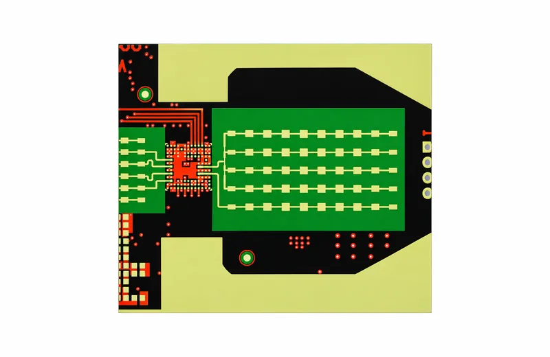
77 GHz hybrid radar
Rogers antenna layers bonded to high-Tg FR-4, with CTE-managed transitions for automotive cycling.
High frequency PCB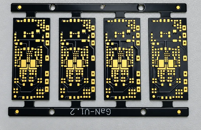
Heavy copper EV inverter
4 oz power layers next to 1 oz impedance-controlled signals, with thermal vias to the heatsink.
Heavy copperThe scenarios below describe typical engineering approaches; the production case studies above are real AstroPCB builds with customer names withheld.
Scenario detail
What each scenario involves.
AI accelerator HDI. A high-layer-count board with stacked microvias for 0.5 mm BGA escape and 90 Ω differential channels for 56G PAM4. The engineering question is how few lamination cycles still route the package. Moving from three-level to two-level stacked microvias can save a cycle per side and a meaningful share of fabrication cost without hurting routing or impedance.
Medical rigid-flex endoscope. A multi-section rigid-flex with thin polyimide flex zones carrying impedance-controlled camera data, dynamic flex endurance for repeated insertion, and Class 3 inspection with lot traceability. Adhesiveless polyimide and rolled-annealed copper maximize flex life.
77 GHz automotive radar. A hybrid stack-up with a low-loss Rogers antenna layer bonded to high-Tg FR-4 for processing and power. The challenge is tight Dk and registration across the antenna and a transition that survives automotive cycling without delamination.
Heavy-copper EV inverter. A 6-layer board with 4 oz power layers carrying high peak current, thermal vias under the gate-driver area to the heatsink, and 1 oz impedance-controlled signal layers next to heavy copper, which needs careful stack-up engineering.
Technology matrix
Technologies by scenario.
| Scenario | Key technologies | Pages |
|---|---|---|
| AI accelerator | HDI, stacked microvias, Megtron, back-drill | HDI · Megtron |
| Medical endoscope | Rigid-flex, polyimide, Class 3 | Rigid-flex · Medical |
| 77 GHz radar | Hybrid Rogers/FR-4, impedance | High frequency · Automotive |
| EV inverter | Heavy copper, thermal vias | Heavy copper · Power |
Engineering approach
How we engage on a complex build.
Complex builds go best when engineering starts before layout is frozen. We usually begin with a stack-up and via-structure proposal for your target layer count and materials, then review placement and breakout once your layout is in progress, then do a full DFM of the released data. That sequence catches the expensive decisions, such as lamination count, material and via type, while they are still easy to change.
Typical outcomes
What early engineering typically changes.
| Early decision | Typical effect |
|---|---|
| Fewer lamination cycles | Lower cost, shorter lead time, better yield |
| Staggered instead of stacked microvias | Better thermal-cycle robustness, lower cost |
| Hybrid instead of all-Rogers stack-up | Lower material cost |
| Right copper weight per layer | Avoids over-plating and spacing problems |
| Correct finish for the package | Fewer assembly defects |
Start a project
How to start a similar project.
- Share a block diagram, target stack-up or reference design
- List fixed requirements: materials, class, certifications
- Send placement or a preliminary layout for early review
- Get a stack-up and via proposal with indicative pricing
- Release final data for full DFM and quote
Early engagement usually costs nothing and is the most effective way to keep a complex board on schedule. Upload files on the quote page or contact engineering.
Our approach
How every project is reviewed.
- Read the data package and fixed requirements
- Check stack-up, materials, vias and copper against the build
- Return written DFM questions before fabrication
- Verify with microsection, TDR and electrical test — free DFM review
FAQ
Common questions.
Can I discuss a similar project?
Yes; contact engineering or upload files for a free DFM review.
Do you sign NDAs?
Yes, before receiving proprietary design data.
Which industries do you serve?
Medical, automotive, aerospace and defense, AI and data center, telecom and power electronics; see industries.
Can you share a sample DFM report?
An anonymized example can be shared on request.
Are these real customer projects?
The five production case studies are real AstroPCB builds; customer names are withheld under NDA. The engineering scenarios describe typical approaches.
Can you share customer names?
Only with written approval from the customer.
Where do the technical values come from?
From the production stack-up drawings and project sheets for each board.
Ready when your files are
Send your design for an engineering review.
Upload Gerber, ODB++ or IPC-2581 data. Every quote includes a written engineering DFM review, typically within one business day.